
Artículo wiki · Colección 04
Tecnología SiC
Referencia técnica sobre Tecnología SiC para el diseño, integración e implementación de sistemas de energía inalámbrica.
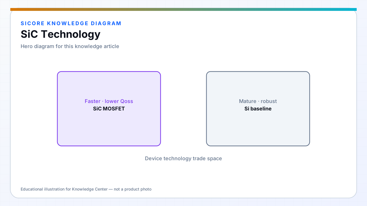
SiC MOSFETs and Schottky diodes excel where voltage stress, temperature, and switching loss intersect — common in multi-kilowatt dock inverters and PFC stages. Lower reverse recovery charge on SiC diodes reduces switching stress on companion switches and can simplify snubber design.
SiC costs have moved toward mainstream industrial power. For 24/7 AGV charging lanes, improved efficiency and cooler operation often justify the premium over Si.
01Typical WPT applications
- Dock inverter full-bridge or half-bridge at 100 kHz and above.
- PFC boost switches in three-phase dock feeds.
- Fast free-wheeling or clamp diodes in hard-switched auxiliary circuits.
02Design differences from Si
SiC MOSFET body diode reverse recovery is generally milder than Si, but short-circuit and avalanche behavior must still be verified. Gate drive voltages and negative bias recommendations vary by vendor — follow the datasheet for turn-off reliability. SiC benefits shrink if conduction loss dominates because RDS(on) is not always lower than optimized Si at the same die size.
03Fleet reliability
- SiC tolerates higher junction temperatures — use that margin for life, not for running hotter by default.
- Qualify gate oxide and threshold drift over production spread.
- Pair with compatible gate drivers rated for SiC Miller plateau.