
Artículo wiki · Colección 09
Diseño Térmico de PCB
Referencia técnica sobre Diseño Térmico de PCB para el diseño, integración e implementación de sistemas de energía inalámbrica.
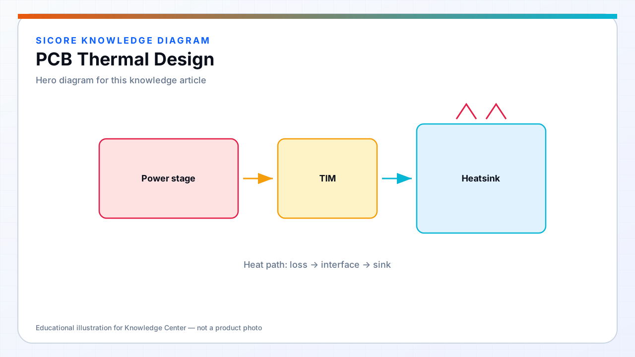
PCBs in wireless charging systems carry both control logic and power: gate driver circuits sit millimeters from half-bridge FETs switching 400 V at 100 kHz, while receiver boards route 80–150 A rectified output through inner layers. Copper is the primary in-plane heat spreader when discrete heatsinks cannot contact every hot device — layout decisions made at schematic capture persist through field thermal performance.
SiCore PCB thermal guidelines apply separately to dock multi-layer power boards ( often 4–8 layers with 2–4 oz outer copper ) and space-constrained receiver boards where 2 oz may be maximum on outer layers due to impedance and cost.
01Copper and via strategy
- Dedicated unbroken copper pours under FET drains and synchronous rectifier low-side FETs tied to thermal via fences.
- Via-in-pad or staggered 0.3 mm thermal vias at 1.0–1.2 mm pitch — filled/plugged when required for assembly yield.
- Split power and return planes to minimize slotting that breaks heat flow from hot center to board edge.
- Heavy-current shunts: Kelvin sense separated from main current path; thermal vias only on non-critical zones.
- Edge connector and mounting hole keep-out zones that do not sever primary spreader paths.

02Component placement and layer stack
Hot FETs cluster along board edge facing heatsink or enclosure wall — not buried center where vias must traverse long distances. Bulk capacitors near FETs reduce loop area and share thermal relief through grounded terminals soldered to large pads. Gate resistors and small-signal parts stay off FET thermal shadow unless elevated on opposite side with via stitching.
Layer stackup documents effective thermal conductivity for simulation: 2 oz outer, 1 oz inner signal, solid GND plane on layer 2 as primary spreader. Receiver boards with aluminum-backed PCB substrate use vendor Rθ values for hot spot under SR FET array — standard FR4 assumptions invalid.
03Validation and production control
Prototype IR scan at rated power identifies trace heating on unexpected neck-down regions — often at fuse holders or sense resistor transitions. Production AOI cannot verify thermal vias; SiCore specifies cross-section audit on first article and X-ray spot check for via fill voids under power FETs. Firmware NTC placement correlates to modeled PCB hotspot within placement tolerance documented on assembly drawing.