
Artículo wiki · Colección 04
Diseño de Etapa de Potencia
Referencia técnica sobre Diseño de Etapa de Potencia para el diseño, integración e implementación de sistemas de energía inalámbrica.
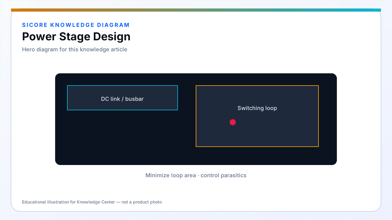
Power stage design is the end-to-end layout of semiconductors, DC link, tank connection, sensing, and cooling that converts bus power into controlled coil excitation. For AGV docks, the stage must fit a floor pad or pedestal, survive environmental stress, and remain serviceable.
A schematic-correct stage fails in production if loop inductance, thermal paths, or clearance rules are ignored.
01Design flow
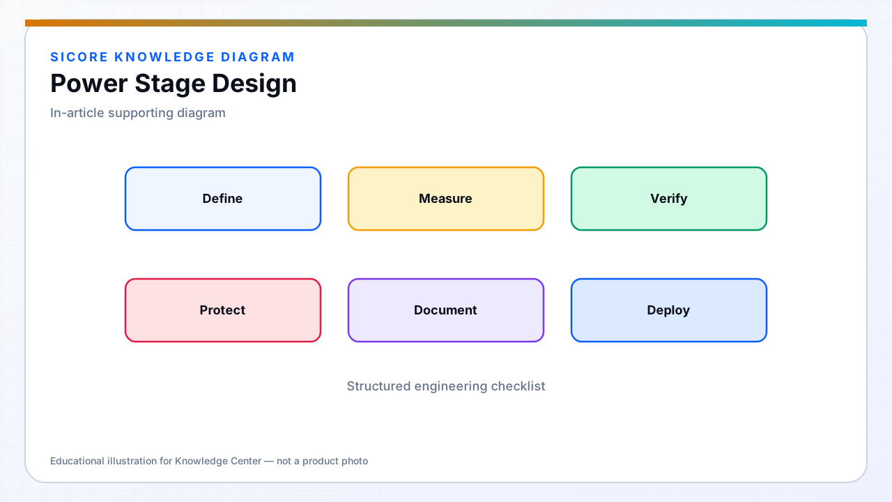
- Define power, frequency, topology, and device technology from system requirements.
- Place switching loop and DC bus capacitors before routing aesthetics.
- Integrate current sense, voltage sense, and temperature monitors at defined points.
- Simulate or measure switching waveforms on first article hardware early.
02Co-stage coupling
The power stage output connects directly to the transmitter coil and resonant network. Impedance at the switch node sets stress on devices and capacitors. Design the stage and tank together — changing compensation without revisiting layout often invalidates ZVS assumptions.
03Manufacturing and service
- Torque specs and thermal interface materials for repeatable assembly.
- Accessible test points for bus voltage, coil current, and gate signals.
- Modular power stage cartridges for field swap in high-uptime deployments.