
Artículo wiki · Colección 03
Apilado de Bobina del Pad
Referencia técnica sobre Apilado de Bobina del Pad para el diseño, integración e implementación de sistemas de energía inalámbrica.

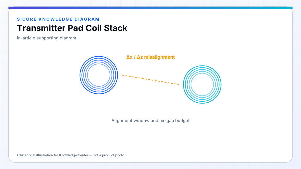
The transmitter pad coil stack orders materials from the charging face downward: wear surface, coil (often litz spiral or DD), ferrite tiles, optional aluminum spreader/shield, structural plate, and cable exit. Each interface adds thermal resistance and shifts L/C through dielectric loading and proximity to conductors.
Floor pads see mechanical abuse — stack design must survive tile compression, forklift crossings (where allowed), and thermal cycling from ambient warehouse to full power.
01Typical layers
- Top: polyurethane or epoxy wear layer (thickness in gap budget).
- Coil: potted or pre-potted assembly on ferrite.
- Ferrite: tiled back-plate with defined gaps.
- Thermal/spreader: aluminum coupling to enclosure or floor.
- Bottom: steel or composite tray with sealed cable gland.
02Integration risks
Metal screws through the stack near the coil create eddy loss and asymmetry — use non-magnetic fasteners or keep them outside the flux path. Reinforcing rebar under cast floors couples flux — pad location vs rebar mesh matters for in-floor installs.
03Service
- Modular coil-ferrite cartridges reduce floor downtime.
- Mark stack version on pad label — mixed revisions in one lane skew power.
- Lift-and-replace procedure for tile without disturbing coil alignment to floor datum.