
Wiki article · Collection 04
GaN Technology
Engineering reference on GaN Technology for wireless power system design, integration, and deployment.
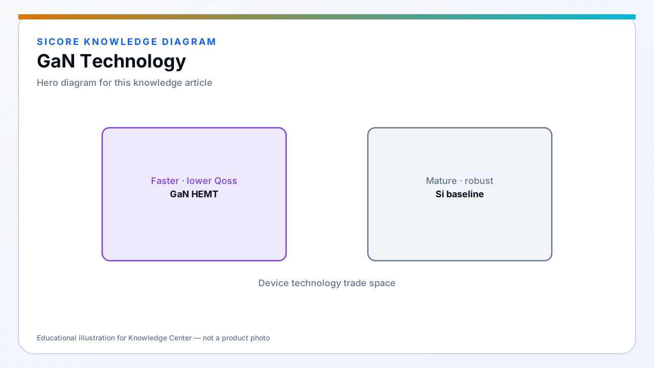
GaN HEMTs offer lower switching loss and smaller device capacitance than comparable silicon MOSFETs, enabling higher frequency or higher power density in the transmitter stage. For floor-mounted charging docks with tight thermal envelopes, that can mean smaller magnetics and heatsinks.
GaN demands disciplined layout — short loops, careful gate drive, and controlled dv/dt. An excellent GaN part on a poor PCB performs worse than a mature Si MOSFET on a good one.
01Advantages for WPT
- Reduced switching loss when pushing frequency for compact coils.
- Lower Qoss aiding ZVS transitions in some topologies.
- Smaller power stage footprint for slim dock profiles.
02Design cautions
Gate threshold and drive requirements differ from Si — use recommended drivers and layout guidelines from the device vendor. Miller plateau and ringing are unforgiving at high dv/dt. EMI filters and shielding may need reinforcement when migrating from Si to GaN at the same frequency.
03When to adopt
- Power density or frequency target cannot be met with Si within thermal budget.
- Team has layout and measurement capability for GHz-speed loop design.
- Total cost of ownership includes magnetics savings, not device price alone.