
Wiki article · Collection 04
Gate Drivers
Engineering reference on Gate Drivers for wireless power system design, integration, and deployment.
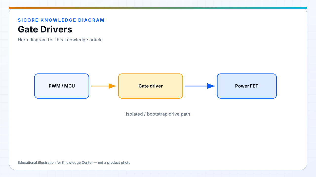
Gate drivers translate low-voltage control signals into the voltage and current needed to charge and discharge MOSFET gates quickly and reliably. In wireless charging inverters, poor gate drive shows up as excessive switching loss, EMI, and unexplained device failures under fast load transients.
Drive capability must match Qg at the operating frequency with margin for Miller plateau. Undersized drive lengthens transition time and moves operation away from soft switching.
01Core requirements
- Peak source and sink current for target rise and fall times.
- UVLO and fault reporting so switches never hang in linear region.
- Matched propagation delay in half-bridge high-side and low-side pairs.
- Isolation when high-side reference floats on the switching node.
02Layout and components
Keep driver close to the FET gate. Use a tight loop for gate resistor, series damping, and optional ferrite. Separate power and signal grounds deliberately — return current from gate discharge must not stamp on sensitive analog or current-sense traces.
03Dock-specific notes
- Gate drive supply must survive pre-charge and idle states without collapse.
- Document replaceable gate resistors for field tuning after EMI audit.
- Test driver performance at minimum and maximum DC bus voltage.