
Wiki article · Collection 03
Ferrite Tile Layout
Engineering reference on Ferrite Tile Layout for wireless power system design, integration, and deployment.
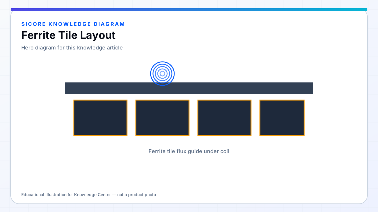
Ferrite tile layout determines how much of the coil back-plane carries guided flux versus fringing into air. Tiles are cut in segments with gaps to limit eddy currents and thermal stress cracks. Incomplete coverage lowers effective permeability; overhang beyond the coil edge can reduce leakage if shaped correctly.
Standard layouts mirror coil outer contour with 2–5 mm gaps between tiles — vendor-specific rules apply for minimum gap and adhesive type.
01Layout variables
- Coverage percentage vs coil OD.
- Gap width and orientation (radial vs circumferential splits).
- Tile thickness vs saturation and weight.
- Central hole sizing for alignment features and cables.
02Assembly
Bond tiles to a flat plate before winding or potting to maintain coplanarity. Warped back-plates create air gaps under ferrite that reduce μ_eff unpredictably. Replace cracked tiles in field service — partial replacement shifts L.
03Testing
- Compare L with full vs 75% tile coverage on samples.
- Thermal imaging for tile hot spots indicating saturation or eddy issues.
- Drop test ferrite assembly before approving layout for AGV impacts.