
Wiki article · Collection 04
Bootstrap Gate Drive
Engineering reference on Bootstrap Gate Drive for wireless power system design, integration, and deployment.
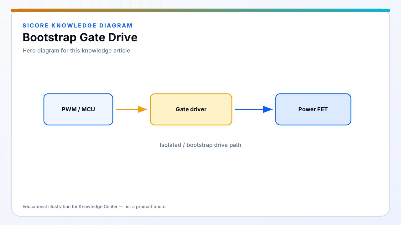
Bootstrap drive charges a capacitor from the low-side supply through a diode while the low side is on, then floats that capacitor on the switching node to drive the high-side MOSFET. It is ubiquitous in half-bridge dock inverters for cost and simplicity.
Bootstrap fails if the high-side on-time is too long without refresh, if the node sits at high voltage too long at startup, or if dV/dt on the node injects noise into the bootstrap pin.
01Design rules
- Size bootstrap cap for gate charge plus quiescent leakage per cycle.
- Limit maximum high-side duty or insert refresh pulses in control.
- Use low-leakage bootstrap diode rated for node voltage plus margin.
02WPT specifics
Resonant operation may create long low-side off intervals — verify bootstrap voltage at light load and during certain phase angles. Multiple switching transitions per period can help or hurt refresh depending on modulation.
03Alternatives
- Isolated DC-DC for high-side when duty cycle or reliability demands.
- Charge pump auxiliaries on integrated gate driver ICs.