
Wiki article · Collection 04
Dead-Time Design
Engineering reference on Dead-Time Design for wireless power system design, integration, and deployment.
6 minArticle 33/50Power Electronics
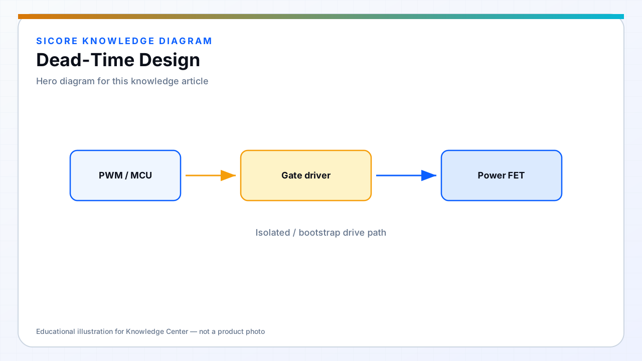
Dead time is the interval when both high-side and low-side switches are commanded off before the opposite device turns on. Too little dead time risks shoot-through; too much forces body-diode conduction and loses ZVS benefit in resonant designs.
Dead time is not a single constant — it may vary with load, temperature, and device spread in production.
01Setting dead time
- Start from driver and MOSFET datasheet recommendations, then adjust on hardware.
- Account for driver propagation mismatch between high and low side.
- Extend dead time when bus voltage or temperature rises if shoot-through margin shrinks.
02Resonant WPT interaction
During dead time, tank current freewheels through body diodes — reverse recovery when the switch turns on creates loss and EMI. Adaptive dead time algorithms use current polarity detection — validate across coupling range.
03Testing
- Scope both gate drives and switch-node voltage simultaneously.
- Production test for gross shoot-through — supply current spikes or fuse indicators.
- Document dead time register values in firmware release notes.