
Wiki article · Collection 04
Parasitic Inductance
Engineering reference on Parasitic Inductance for wireless power system design, integration, and deployment.
6 minArticle 48/50Power Electronics
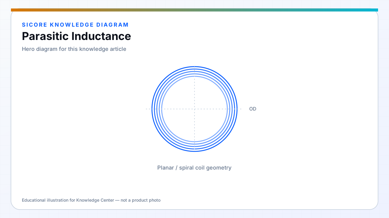
Parasitic inductance in switch loops, DC bus, and rectifier connections stores energy that rings at turn-off. It scales with loop area and path length — the enemy of clean waveforms in compact receiver boards and floor pad modules.
A schematic with ideal wires hides nanohenries that push VDS beyond rating.
01Sources
- Long traces between cap and FET, or FET and coil terminal.
- Connector pins and wire bonds in package.
- Asymmetric return path forcing current around large loops.
02Mitigation
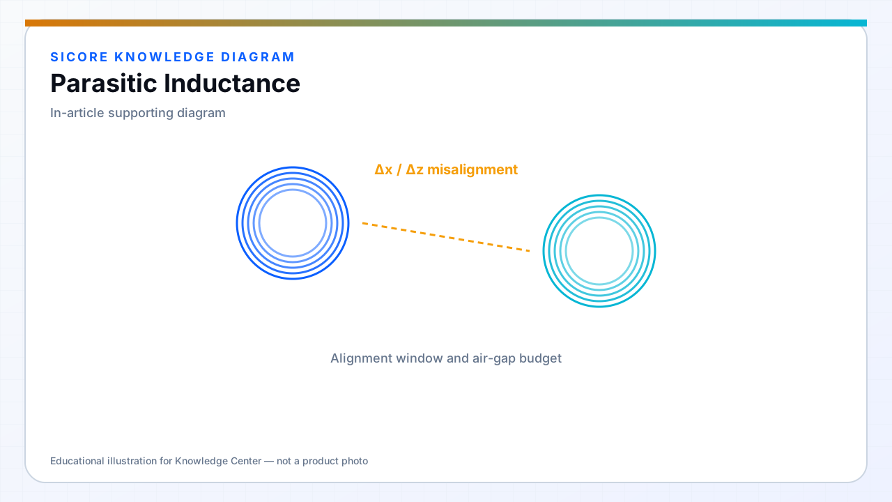
Co-locate components; use plane returns; parallel vias; optional snubber only after minimizing L. Measure loop inductance with impedance analyzer or step response.
03WPT impact
- Ringing detunes effective tank behavior sensed by control.
- EMI peaks at ring frequency — filter may not help if source L is large.